In our earlier article about the production cycle of solar panels we provided a general outline of the standard procedure for making solar PV modules from the second most abundant mineral on earth – quartz.. In
While total photovoltaic energy production is minuscule, it is likely to increase as fossil fuel resources shrink. In fact, calculations based on the world''s projected energy consumption by 2030 suggest that global energy
Screen-printed solar cells were first developed in the 1970''s. As such, they are the best established, most mature solar cell fabrication technology, and screen-printed solar cells currently dominate the market for terrestrial photovoltaic
isotropic chemical etching based on defects rather than crystal orientation 6; isotropic chemical etching in combination with a photolithographic mask 7, 8; plasma etching 9. Antireflection Coatings and Fire Through Contacts
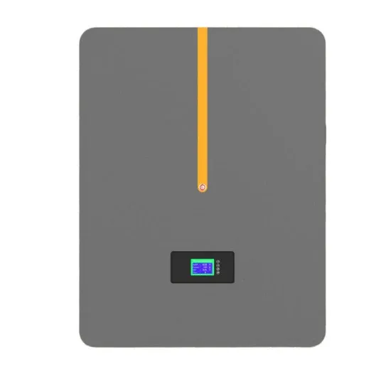
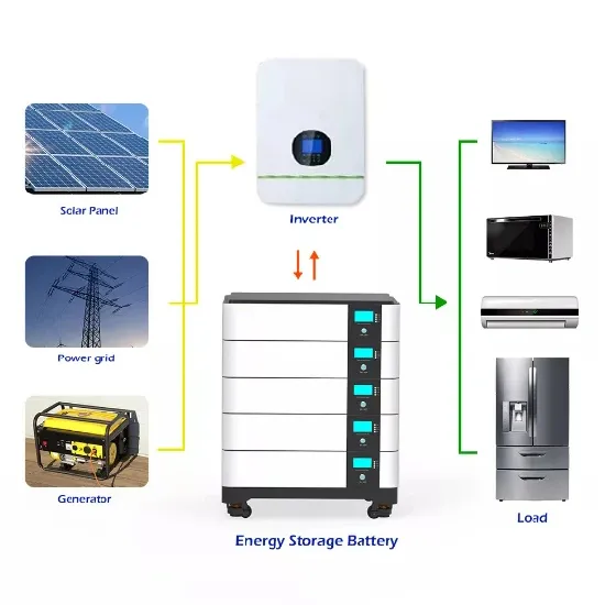
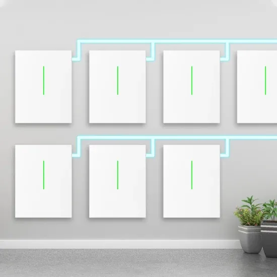
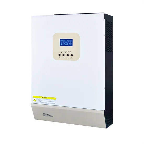
Working of the solar panel system. The solar panel system is a photovoltaic system that uses solar energy to produce electricity. A typical solar panel system consists of four main components: solar panels, an inverter, an
The photovoltaic principle is the cornerstone of how solar cells convert solar energy into usable electricity. While silicon solar cells dominate the market, novel materials are evolving and showing promise in enhancing solar
The first etching process resulted in deep grooves, 36 μm on average, on the front of recycled wafers that rendered the process unsuitable for wafers to be used in solar cell production. Such grooves occurred due to different etching
1 Introduction. Plasma-enhanced chemical vapor deposition (PECVD) of thin film silicon is a key process in various industrial applications. Thin film silicon material is used in flat panel displays
The objective of the etching and edge isolation process is to remove this electrical path around the wafer edge by disk stacking the cells on top of each other and then exposing them to a plasma etching chamber using
r is the yield of the solar panel given by the ratio : electrical power (in kWp) of one solar panel divided by the area of one panel. Example : the solar panel yield of a PV module of 250 Wp
For example, with a standard string inverter, if one solar panel produces less energy, all the solar panels in that string will produce less energy. With the power optimizer, each solar panel
Etching is a process which removes material from a solid (e.g., semiconductor or metal). The etching process can be physical and/or chemical, wet or dry, and isotropic or anisotropic. All these etch process variations can be used during solar cell processing.
Etching process is a commonly adopted technique used in the fabrication of black silicon. Etching processes for black silicon fabrication include electrochemical etching, stain etching, and metal-assisted chemical etching [26, 27, 28, 29, 30].
Both the groups used standard alkaline (KOH based) etching process (after the SDR process) for texturing the DWS c-Si wafer surface. The solar cell performance parameters of their DWS c-Si cells were similar to that of the conventional saw damage etched and alkaline textured MWSS c-Si cells .
The typical etch rates are 2-4 µm/min at 6-10 °C. Due to the different grain orientations within the same multicrystalline silicon wafer, acidic etching is used to texture this type of material. Acidic solutions are also used to perform defect etching (e.g. Sopori etching ).
Physical etching or sputtering is a dry process where the material is removed due to ion bombardment. The ion bombardment is delivered by a plasma. This process is known to : be chemically unselective – depends only on the surface binding energy and the masses of the targets and projectiles,
Acidic etching is performed at low temperatures (6-20 °C) and is normally isotropic. The typical etch rates are 2-4 µm/min at 6-10 °C. Due to the different grain orientations within the same multicrystalline silicon wafer, acidic etching is used to texture this type of material.